Introduction
The goals and needs of today’s computer hardware customer are more diverse than ever before. Some people have a need for speed. Some will not buy a motherboard unless it has a list of specific features that he or she believes will be required for future upgrades. Others shy away from the cutting edge, instead requiring time-tested stability in a motherboard. Whether you are an over-clocker trying to squeeze the last MHz out of a CPU, or an IS manager who is looking for a corporate motherboard, you have to understand a motherboard’s chipset.
This article will address popular chipsets for the most commonly used modern CPUs: Intel’s Celeron and Pentium 4 and AMD’s Duron and Athlon XP.
| Go To Top |
What is a chipset?
A motherboard chipset has both a general definition and a specific definition that varies by chipset manufacturer. Generally speaking, a motherboard chipset controls the features and abilities of the motherboard. If you understand which chipset a motherboard uses, you know a good deal about its potential features and abilities before ever reading the motherboard’s specifications.
Modern motherboard chipsets nearly always consist of two separate chips. These two chips on the motherboard are called the north bridge and the south bridge. Together, the north bridge and the south bridge handle all of the communication between the processor, RAM, video options, PCI slots, BIOS, ATA controller, USB ports, integrated modem, integrated LAN port and integrated sound. The chipset also determines the type of RAM that can be used.
There are a dozen or so reputable motherboard manufacturers and about a half dozen popular chipset manufacturers. Intel and AMD provide specifications to the chipset manufacturers, who, in turn, develop and sell chipsets with various features and abilities to motherboard manufacturers. Of course, the exceptions to this are Intel and AMD, who also create their own chipsets.
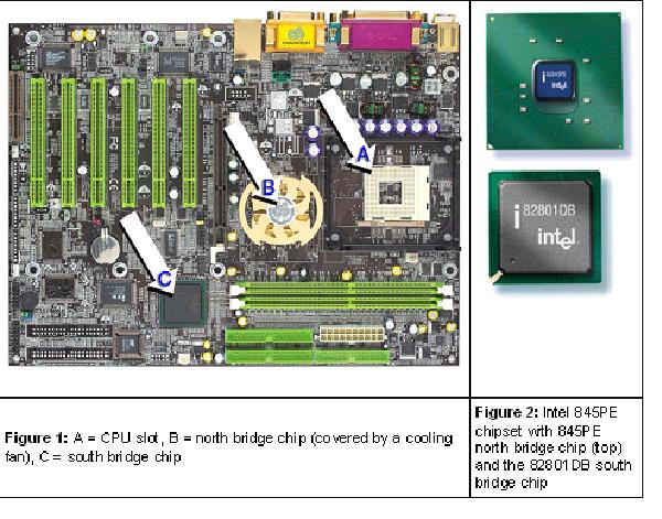
The North Bridge
Front-Side Bus Speed
The north bridge controls the communication and throughput speed between AGP video, the RAM and the CPU. The speed at which the memory can communicate with the CPU is referred to as the front-side bus speed or system bus speed. For those who are looking for ultimate speed, the north bridge’s front-side bus speed is a key item to study. If you want a fast CPU and fast RAM, you need a fast front-side bus. Modern CPUs and RAM come in a variety of ratings for front-side bus speeds and must be matched with an appropriate chipset (which determines the motherboard’s front-side bus speed). A speed mismatch will create a performance bottleneck.
For example, RAM can be purchased in a variety of speeds such as DDR200, DDR266, DDR333, or DDR400. Each number next to “DDR” represents a frequency speed rating. DDR266 should only be used with a front-side bus of at least 266MHz, and DDR400 requires at least a front-side bus speed of 400MHz. When the front-side bus speed is the same as the speed of the DDR RAM, this combination is described as being “synchronous.” It is the motherboard chipset (within the north bridge) that specifies the front-side bus speed. See the glossary section for additional information on DDR speeds.
Sometimes a chipset will specify asynchronous combinations of front-side bus speed and RAM speed, such as allowing DDR400 to be used with a front-side bus speed of only 333MHz. Benefits from these asynchronous combinations usually require overclocking the front-side bus.
Modern Pentium 4 chipsets run at either 100MHz or 133MHz clock cycles. However, they are quad pumped (also known as quad data rate). Therefore, the front-side bus speeds are 400MHz or 533MHz. To explain quad pumping – If a quad pumping 133MHz system bus were a car analogy, it would be analogous to taking a single 133MHz lane, and instead providing four 133MHz lanes of traffic.
AMD chipsets are similar, except that they operate at either 100MHz, 133MHz or 166MHz. AMD chipsets are double pumped (versus Intel’s quad pumped). Therefore, the front-side bus operates at effective speeds of 200MHz, 266MHz or 333MHz respectively. However, do not be misled by the MHz rating of the chipset. While MHz is still important, it is no longer the sole determiner of system performance.
If we carry our car analogy further and compare MHz to horsepower, one car may have more horsepower but have a less efficient fuel system. It is possible for a car that has a more efficient fuel system to run as fast as a car with more horsepower. This is the case when comparing Pentium 4 and AMD chipsets. Intel’s CPU and chipset runs at a higher total MHz than AMD’s. However, AMD’s CPU and chipset can run just as fast because it has higher efficiency (Specifically, In some scenarios, AMD is better at speculative branch predictions, which can increase the number of instructions per clock cycle). This is the reason that AMD moved from identifying its processors by their megahertz rating to a name identified with a specific number. The identifying number is meant to show that it is as fast as the corresponding Pentium 4. For example, the Althon XP 2700+ operates at 2166MHz; however, AMD asserts that it operates as fast as the Pentium 2.7GHz.
For more detailed information regarding front-side bus speeds, review Directron’s article by Lee Penrod, “Understanding System Memory and CPU speeds: A layman’s guide to the Front Side Bus (FSB).”
AGP Speed The north bridge also controls the speed at which information is exchanged with the AGP video slot. In September of 2002, Intel released the final version of the AGP standard – AGP 3.0. This moved the available speed of AGP video from 4X to 8X. AGP 8X can move data at twice the speed of AGP 4X. While most people want fast AGP for gaming reasons, as of this writing (March 2003), there are no games available that can provide enough data to take advantage of AGP 8X. If you are deciding on which chipset to choose based on whether or not it supports AGP 8X, just understand that it may be a year or so before you will realize the fruits of this chipset capability.
Some north bridges have integrated graphics. In other words, you do not need to buy a separate video card. Video is built into the motherboard in the north bridge chipset. This option is usually targeted toward the budget-conscious consumer who does not care whether or not a PC’s graphics system can handle Unreal Tournament 2003. On the other hand, a few chipsets with integrated graphics have above average graphics-handling power, such as the nForce2 IGP chipset.
The South Bridge
The south bridge is often referred to as the I/O controller. The features of the south bridge change less often than the those of the north bridge. From chipset to chipset, nearly all south bridges have support for integrated sound, LAN and modem, ATA and USB. However, just because a chipset can support these features does not mean that the motherboard manufacturer will make that particular feature available. There are also some I/O components that are not controlled by current south bridges, such as RAID and Serial ATA. These have their own chips, separate from current north and south bridges. This will change in the future, as Intel is incorporating Serial ATA into their upcoming Springdale chipset.
When a chipset manufacturer releases a new chipset, it is common for the north bridge to change, while the south bridge may remain the same as the one used previously. There are two notable south-bridge controlled items that have changed over the last few generations of chipsets: USB 2.0 and ATA 133.
USB 2.0
USB 2.0 is forty times faster than USB 1.1, it is hardware dependent (the hardware must be USB 2.0 compatible) and it requires an operating system that supports it. For example, even if you are running Windows XP, you must have service pack one installed in order to utilize USB 2.0. If you want USB 2.0, and you find a chipset you like that has everything except USB 2.0, you can always add a PCI card with USB 2.0 support fairly inexpensively.
ATA is the IDE controller of the south bridge. It controls your hard disk, CD/DVD drives, and any other IDE device. Modern chipsets all support ATA 100, and some support ATA 133. The number after “ATA” represents, in theory, the amount of data in MB/second that can be transferred between your IDE device and the south bridge. Therefore, ATA 100 has a data throughput of 100MB/second and ATA 133 has a data throughput of 133MB/second.
ATA 133 is a standard that was developed by Maxtor in 2001. Maxtor holds the license for ATA 133, and they want to charge other hard disk manufacturers for the right to use this technology. Currently, Maxtor is the only hard disk manufacturer that is producing hard disks with ATA 133 compatibilities. There are several reasons that other hard disk manufacturers have not adopted ATA 133. One reason is that Serial ATA hard disks are now becoming available. Serial ATA has a data throughput of 150MB/second. Once Intel incorporates Serial ATA into its chipset, hard disk manufacturers will have even fewer reasons to license ATA133 from Maxtor.
Another reason is that data throughput speeds of the ATA 133 drives are being matched by ATA 100 hard disks with various configurations such as an 8MB cache. Also, the additional 33% bandwidth of ATA 133 is more of a benefit when sudden bursts of data are required. It quickly loses its efficiency over sustained transfers of data.
ATA 133 used to have a capacity advantage over ATA100. The ATA 100 hard disks were limited to 137GB. However, in 2001, a standard was developed that allowed hard disks to utilize 48-bit logical block addressing. This removed the 137GB barrier to ATA100 hard disks. ATA hard disks with 48-bit addressing started appearing in 2002.
To summarize ATA 133, unless you have a very specific Maxtor hard disk you are looking to support, ATA 133 should not rank high on your chipset selection criteria list.
Audio Support in the South Bridge
Another way chipset manufacturers have differentiated their south bridge is by enhancing the audio support. Most modern chipsets support six-channel audio (two front speakers, two rear surround channels, a center channel and a subwoofer). The motherboard manufacturer may or may not provide six separate speaker connections, but the support is there for it in the chipset. In addition, some chipset manufacturers, like nVidia, are incorporating AC3 (Dolby Digital) 5.1 encoding into the south bridge.
| Go To Top |
Chipset Manufacturers
On the Pentium 4 side, the most popular chipset manufacturers are Intel, SiS and VIA. On the AMD side, the prominent chipset manufacturers are SiS, VIA, nVidia, AMD and ALi.
Earlier, it was mentioned that chipset manufacturers have their own specific way of naming and articulating the features of their chipsets. Most chipset manufacturers will use the name of their north bridge as the name for the entire chipset, even though the south bridge has its own name. However, this is not always the case. For example, VIA’s KT133A used a north bridge named VT8363A. Other chipset makers eschew the customary alphanumeric chipset name, and, instead, opt for a marketing name such as nForce. The north bridge usually gets the lime light; that is where the power lives. Advancing the features of the north bridge is what drives the release of a new chipset. In fact, it is not uncommon for a chipset to have its south bridge updated without changing the name of the chipset. For example, a chipset manufacturer may extend the life of a chipset by updating the south bridge to include ATA 133 and/or USB 2.0.
Not too long ago in the months between 2001 and mid 2002, the chipset market was dominated by VIA and Intel. However, recently, VIA has lost a dramatic amount of market share. SiS is now the second largest distributor of chipsets, with Intel still holding a dominant position distributing its own chipsets. For the various 3rd-party chipset manufacturers, market share is largely dependent on whether you develop chipsets for AMD, Intel or both. Intel, however, can dominate the chipset market even though they do not develop AMD chipsets because, as of this writing, Intel has nearly 85% of the desktop, laptop and server market. AMD has about 14% of total CPU market share (see Figure 4).
VIA
VIA has a long history of chipset development, and they have made fans and enemies along the way. A few years ago, VIA released a south bridge (686B) with PCI latency issues that caused havoc with sound cards, especially Creative Labs SoundBlaster cards (which were very popular cards at the time). This gave VIA a bad name that lingers with some people, still long after the issue was resolved. All chipsets have hardware hiccups from time to time, and this was not VIA’s last, but it continues to be very memorable to many.
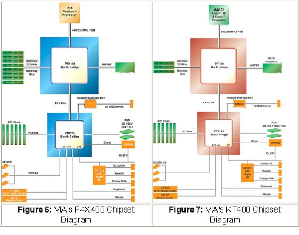
Most recently, VIA has been wrestling with Intel over bus licensing rights that would allow them to advertise their 533MHz Pentium 4 chipset, P4X400, as supporting hyper-threading. VIA is claiming that Intel is using unfair competitive practices. This clash with Intel caused very few motherboard manufacturers to use the P4X400 initially. The licensing issue resolution has not been made public; however, VIA is now advertising hyper-threading support for the P4X400 chipset. VIA’s Pentium 4 chipset, P4X400, is very competitive, offering support for the 533MHz front-side bus, DDR400 and AGP 8X.
On the AMD side, the VIA KT400 has been a success. The KT400 supports the fastest front-side bus possible for the AMD at 333MHz and AGP 8X, as well as the latest features in the south bridge, supporting USB 2.0 and ATA 133. However, VIA feels the pressure being presented by nVidia’s nForce 2 line of chipsets that sport dual 64-bit memory controllers, allowing the use of dual-channel DDR configurations. Recently (March 2003), VIA announced an update to the KT400 chipset, calling it the KT400A.
The KT400A comes equipped with enhancements to the memory controller that VIA calls FastStream64? This enhanced memory controller offers ten percent improvement in 3D applications over the previous KT400 chipset, and it officially supports DDR400. It also offers native support for serial ATA when combined with the VT8237 south bridge. If KT400A motherboards equipped with the VT8237 south bridge hit the streets before motherboards with Intel’s Springdale chipset, they will be the first motherboards to support native serial ATA in the chipset.
Chipset manufacturers generally rely on motherboard manufacturers to provide direct technical support to end users. This is true for VIA as well. However, VIA does have a well-used forum for discussing chipset related problems called the VIA Arena.
SiS
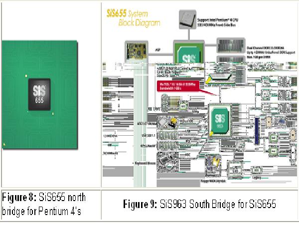
SiS is aggressively pursuing the PC enthusiast market, and has just released a new chipset for the Pentium 4 called the SiS655. It provides dual-channel DDR support, AGP 8X, USB 2.0 and integrated IEEE1394a. Dual-channel DDR means that the north bridge memory controller will read from two DDR DIMMs at the same time, doubling (in theory) the maximum memory bandwidth capabilities. This chipset will compete with Intel’s new E7205 chipset, which also supports dual-channel DDR. However, the SiS655 chipset supports dual-channel DDR333, while Intel’s E7205 only specifies DDR266 for dual-channel use.
SiS is often first on the chipset scene with new features and abilities. This time, they beat VIA to market for a dual-channel DDR solution. VIA will soon have the P4X600 chipset available to support dual-channel DDR.
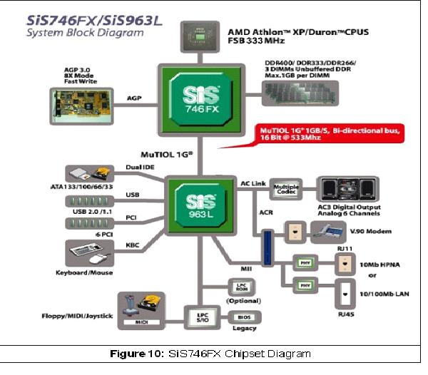
SiS’ latest AMD chipset is the SiS746FX. It supports 333MHz front-side bus, AGP 8X, USB 2.0 and ATA 133. One thing that is interesting about this release by SiS is that SiS is suggesting that you can use DDR400 with it. The following is from SiS’ website: “The SiS 746FX DDR-400 memory controller delivering 3.2G/B bandwidth way adequate and satisfactory to the 333MHz S2K FSB bandwidth demand of 2.7 GB/s, absolutely brings out the best performance of each other, and still has a lot to spare for the multi-I/O masters, and AGP-8X masters.”
Cutting through the hype and awkward sentences that are obviously composed by non-English speaking writers, a stock installation with a 333MHz front-side bus will not take full advantage of the bandwidth DDR400 has to offer. However, the additional DDR bandwidth may appeal to those who like to overclock the front-side bus.
SiS’ Latest Intel Chipset: SiS655
SiS’ Latest AMD K7 Chipset: SiS647FX
nVidia (AMD only)
nVidia has only been in the desktop chipset business for a couple of years, but they have quickly won a lot of enthusiastic fans in the AMD community. Being one of the most powerful names in desktop graphics, nVidia is no stranger to PC consumers. If you asked the average gaming enthusiast if he or she would like to have the same chipset in his or her computer that runs in Microsoft’s Xbox, you would likely perk the gamer’s attention. Of course, nVidia has had its chipset in the Xbox for over two years now.
Current nVidia nForce2 Choices
nForce2 IGP-MCP Dual 64-bit memory controllers, Integrated graphics using GeForce 4 MX and regular AC’97 integrated sound.
nForce2 IGP-MCP-T Dual 64-bit memory controllers, Integrated graphics using GeForce 4 MX and Dolby Digital 5.1 encoding
nForce2 SPP-MCP Dual 64-bit memory controllers and regular AC’97 integrated sound.
nForce2 SPP-MCP-T Dual 64-bit memory controllers and regular and Dolby Digital 5.1 encoding
Original nVidia nForce Choices
nForce 420-D Dual 64-bit memory controllers, Integrated graphics using GeForce 2 MX and Dolby Digital 5.1 encoding
nForce 415-D Dual 64-bit memory controllers and Dolby Digital 5.1 encoding
nForce 220-D Single 64-bit memory controller, Integrated graphics using GeForce 2 MX and Dolby Digital 5.1 encoding
nForce 220 Single 64-bit memory controller and regular AC’97 integrated sound.
Figure 11: nVidia nForce2 and original nForce chipset features
nVidia’s newest chipset for the desktop PC, the nForce2, offers motherboard manufactures a choice of four combinations for the north bridge and south bridge. The nForce2 builds on features of the original nForce chipset. The nForce2 has a choice of two north bridges: SPP and IGP. It also has two choices for the south bridge: MCP and MCP-T. These north and south bridges can be mixed and matched.
The main difference between the nForce2 SPP and the IGP is integrated graphics. SPP stands for Systems Platform Processor, and IGP stands for Integrated Graphics Processor. Both north bridges support dual-channel DDR with dual 64-bit memory controllers. Both support the option of AGP 8X. However, the IGP north bridge has an integrated GeForce 4 MX.
MCP stands for Media and Communications Processor. The MCP and MCP-T south bridges both offer ATA 133, USB 2.0, LAN and integrated audio. The MCP-T extends the features offering to include Dolby Digital 5.1 encoding, IEEE1394a and DualNet (two network controllers). The “T” in MCP-T stands for “Turbo”, which refers to “more features” not “speed.”
Currently, nVidia is only making chipsets for AMD CPU’s. This probably suits Intel, SiS and VIA just fine, as nVidia is quickly capturing market share in the AMD community. When nVidia approached Intel regarding developing chipsets for the Pentium 4, Intel’s response was a licensing fee that made it very unattractive for nVidia.
An oddity that justifies mentioning is a slight naming convention difference for the nForce2 chipset from motherboard manufacturer to motherboard manufacturer. Some refer to the nForce2 south bridge as MCP and MCP-T and others use MCP2 and MCP2-T. For example, Abit and MSI refer to the nForce2 south bridge as MCP2 and MCP2-T. While Asus, EPoX, Chaintech, Leadtek, and Soltek call the nForce2 south bridge MCP and MCP-T. The reasoning for this is unclear; however, there are no differences within the nForce2 chipset that are identified by adding a “2” to the south bridge name. The danger is that someone might choose, for example, an MSI nForce2 MCP2-T motherboard over an Asus nForce2 MCP-T motherboard – thinking that the MCP2-T is more current or has more features than the MCP-T. This is not the case. It can further be confused by the fact the original nForce chipset referred to its south bridge as MCP and MCP-D. Of course, there is a difference between the nForce MCP and MCP-D and the nForce2 MCP and MCP-T.
Intel
Intel is still king of the chipset hill for market share. For years, Intel has made a reputation of creating stable chipsets. Generally speaking, if you are looking for the ultimate in stability, you should investigate an Intel motherboard, which, of course, will have an Intel chipset. When you want the latest cutting-edge gaming features, like AGP 8X, you should see what is being offered by other chipset makers. Intel’s conservative approach can be illustrated by the fact that, even though there is a Intel chipset supporting AGP 8X (the E7205), there is not yet an Intel motherboard supporting AGP 8X (as of this writing). Others, such as the motherboard manufacturer Gigabyte, have taken the Intel E7205 chipset and created the GA8INXP motherboard with AGP 8X. However, Intel has yet to release such a motherboard.
Saying Intel is conservative is not saying that their chipsets produce motherboards that are performance slouches. In fact, if you research which Pentium 4 motherboards are best for overclocking, you will usually find a 3rd-party manufacturer, such as Abit and Asus, using an Intel chipset.
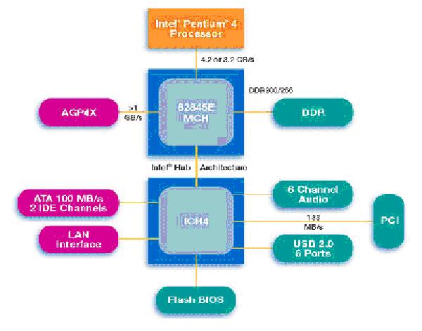
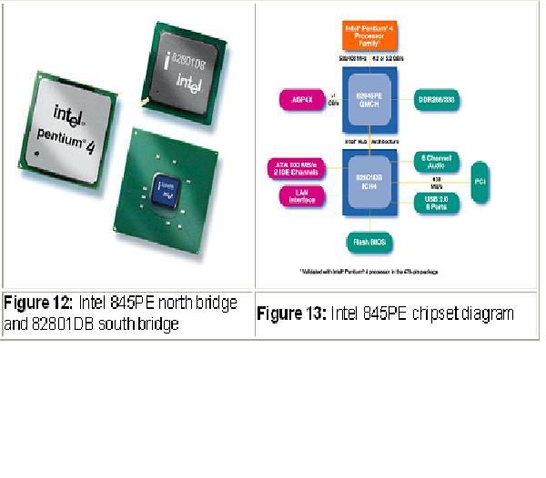
Intel’s latest desktop motherboard chipset is the 845PE, which supports a 533MHz front-side bus, Hyper-Threading, AGP 4X and DDR333. Its south bridge supports the usual south bridge inclusions and USB 2.0 and ATA 100. All of the Intel chipsets with a 533MHz front-side bus support hyper-threading.
Intel’s E7205 is technically designated as a workstation chipset. However, gaming enthusiast and those in search of the fastest desktop system with an Intel chipset are happily using E7205 motherboards, such as the GA8INXP motherboard, in home systems. So, in that sense, you could say that the E7205 is actually the latest Intel desktop chipset.
Figure 14: Intel E7205 chipset
One of the most exciting things about the E7205 is that it supports dual-channel DDR. However, the fastest RAM supported by the chipset is DDR266. Later this year, Intel will release the Springdale chipset that will support dual-channel DDR400 with an 800MHz front-side bus.
| Go To Top |
Summary
It is important to realize that chipsets are not like your motherboard BIOS, which can be updated to add features. Chipsets are not like a CPU chip, which can be removed and changed. Chipsets cannot be updated without replacing the motherboard. You need to understand the features and capabilities of a motherboard’s chipset to make sure that your goals are going to be met. If you are on a budget, you might look for a chipset that has integrated graphics in the north bridge and integrated sound, modem and LAN in the south bridge. If you are looking for a gaming screamer, you need to understand the supported front-side bus speed and whether or not AGP 8X is important to you.
Study the chipset matrixes at the bottom of this article to see differences at a glance.
Glossary
AC’ 97 Intel specifications for adding audio codecs to a chipset (AC is an abbreviation for “audio codec”).
ACR Advanced Communications Riser. ACR describes a riser card that plugs into a special slot on the motherboard (called an ACR Slot). This card provides options, such as modem and sound connections.
Athlon AMD’s Socket A CPU. It has a 200 or 266MHz front-side bus and an L2 cache of either 256KB or 512KB. It currently exists in versions from 500MHz to 1.4GHz.
Athlon XP AMD’s Socket A CPU. It has a 266MHz or 333MHz front-side bus and an L2 cache of either 256KB or 512KB. It’s currently available in versions 1200MHz to 2250MHz. However, the CPU is identified with a number that relates to its corresponding speed with Intel’s P4 CPU. For example, the Althon XP 2700+ operates at 2.16GHz; however, AMD asserts that it operates as fast as the Pentium 4 2.7GHz.
Barton AMD’s development name for the Athlon XP 0.13 micron CPU with an L2 cache of 512KB.
Crush 11 nVidia’s development name for nForce 220
Crush 12 nVidia’s development name for nForce 415 and 420
Crush 18 nVidia’s development name for nForce2
Crush K8 nVidia’s development name for the chipset for AMD’s Clawhammer (also known as Hammer)
DDR1600 or PC1600 Same as DDR200, which means that it works with a front-side bus that is at least 200MHz. The “1600” refers to the amount of data in MB/s that it can transfer.
DDR2100 or PC2100 Same as DDR266, which means that it works with a front-side bus that is at least 266MHz. The “2100” refers to the amount of data in MB/s that it can transfer.
DDR2700 or PC2700 Same as DDR333, which means that it works with a front-side bus that is at least 333MHz. The “2700” refers to the amount of data in MB/s (2666 MB/s) that it can transfer.
DDR3200 or PC3200 Same as DDR400, which means that it works with a front-side bus that is at least 333MHz. The “3200” refers to the amount of data in MB/s (3200 MB/s) that it can transfer.
DualDDR nVidia’s term to describe how its north bridge contains dual 64-bit memory controllers, which creates a 128-bit wide DDR channel to support dual-channel DDR configurations. This was called TwinBank with the release of the nForce chipset, and it was changed to DualDDR with the release of nForce2.
Duron AMD’s Socket A CPU. It has a 200MHz front-side bus and a 64KB L2 cache. It currently exists in versions from 600MHz to 1.3GHz.
Hyper-Threading Intel’s term to describe a processor’s ability to simultaneously process multiple threads of execution. Stated simply, it allows one processor to function as it there were two processors installed.
HyperTransport AMD’s term to describe the communication channel between the north and south bridge. nVidia also uses AMD’s HyperTransport technology in their nForce / nForce2 chipsets. ALi is using HyperTransport in their M1687 north bridge for the AMD K8 CPU.
I/O Controller Hub Another way to refer to the south bridge (especially used by Intel)
IGP nVidia’s acronym for its nForce/nForce2 north bridge with integrated GeForce 2 MX / GeForce 4 MX. It stands for Integrated Graphics Processor. IGP-128 means that it has two 64-bit memory controllers. IGP-64 means that it has one 64-bit memory controller.
K7 K7 is AMD’s code name for the Athlon (including Athlon XP). K8 will be Athlon 64, also known as the Hammer or Clawhammer.
MCH Memory Control Hub – associated with the north bridge’s control of memory data exchanged with the CPU.
MCP NVidia’s acronym to describe its south bridge. It stands for Media and Communications Processor. In the nForce series, MCP-D means that it has digital sound capabilities. In the nForce2 series, the digital sound is identified as being the MCP-T south bridge. The “T” stands for Turbo (not because of speed, but because of additional features).
MicroATX A smaller motherboard than the ATX-style, with a maximum size of 9.6″ square. It will have no more than 4 expansion slots, whereas ATX can have up to 7.
Palomino AMD’s development name for their 0.18 micron CPU with an L2 cache of 256K.
S/PDIF S/PDIF stands for Sony/Philips Digital Interface. It is most commonly used in reference to the cabling needed to connect to a motherboard that supplies digital sound.
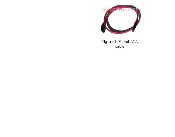
Serial ATA Serial ATA uses a narrow serial link cable to connect the hard disk to the motherboard. The first-generation of this new standard has a transfer rate of 150MB/second. Another benefit is that it is not limited to 18 inches in length, like current IDE cables. Serial ATA cables can be up to 1 meter (3.3 feet).
Slot 1 Intel’s CPU on a card design that plugs into a slot on the motherboard. Supports Pentium II, III and some Celeron CPU’s.
Slot A AMD’s CPU on a card design that plugs into a slot on the motherboard. It supported early Athlon and Thunderbirds.
Socket 370 Intel’s CPU design supporting low-end Celerons and early P4s with 370 pins
Socket A AMD’s CPU specification to support their Duron and Athlon CPUs. Also known as Socket 462.
SPP NVidia’s acronym to describe its north bridge that does not have integrated graphics. It stands for Systems Platform Processor.
Stepping Stepping refers to a CPU’s development version. It starts at A0 (A zero) and increments alphanumerically. For example, A0, A1, A2.
System Bus The system bus is the interface between the north bridge’s memory controller and the processor. The bandwidth and speed of the system bus is measured in megahertz (MHz). It is also called the Front Side Bus.
Thoroughbred AMD’s development name for their Athlon XP 0.13 micron CPU with an L2 cache of 256K.
USB 2.0 USB 2.0 is a new standard for USB that is 40 times faster than USB 1.1. It requires compatible hardware and an operating system that supports it. Windows XP requires SP1 to support USB 2.0.
| Go To Top |
Intel Chipsets
Chipset (by release date) P4 / Celeron Supported North Bridge Fastest FSB Fastest AGP Sup-ported RAM Supported Dual Channel DDR or Rambus Memory Modules Max RAM Sup-ported Max Memory Bandwidth Per Second Sup-ports Hyper-Thread-ing South Bridge PCI Slots Fast-est USB Fastest ATA sup-ported Marketing Claim Sound Bite Release Date Misc. Comments
Intel
E7205
478-pin P4 E7205 533MHz 8X DDR 200 / 266 Yes 4 DDR DIMMs 4GB 4.3GBps Yes 82801DB
6 USB 2.0 ATA 100 …supports USB 2.0 and are the first from Intel to include support for AGP 8x, which provides twice as much bandwidth as AGP 4x, for graphics intensive applications. Nov-02
845PE
478-pin P4 or Celeron 82845PE 533MHz 4X DDR 333 / 266 No 2 DDR DIMMS 2GB 4.2GBps Yes 82801DB
6 USB 2.0 ATA 100 …the newest discreet graphics chipset developed with DDR333 Oct-02
845GV
478-pin P4 or Celeron 82845GV 533MHz N/A DDR 266 / 200 / PC133 SDRAM No 2 DDR DIMMS or 2 SDRAM DIMMs 2GB 4.2GBps Yes 82801DB
6 USB 2.0 ATA 100 …the flexibility to support 533/400 MHz system bus speeds and DDR266/200 memory, while maintaining backward-compatibility with PC133 SDRAM Oct-02
Integrated Graphics and no AGP support
845GE
478-pin P4 or Celeron 82845GE 533MHz 4X DDR 333 / 266 No 2 DDR DIMMS or 3 SDRAM DIMMs 2GB 4.2GBps Yes 82801DB
6 USB 2.0 ATA 100 “Added support for DDR333 main memory further improves both graphics and system performance.” Oct-02
Integrated graphics and also has AGP 4X
850E
478-pin P4 or Celeron 82850E
533MHz 4X Rambus / PC1066 / PC800-40 / PC800-45 Yes 4 RIMMs 2GB 4.2GBps Yes 82801BA
6 USB 1.1 ATA 100 …extends the capabilities of the Intel?850 chipset platform by adding 533 MHz system bus and PC1066… Oct-02
845E
478-pin P4 or Celeron 82845E
533MHz 4X DDR 266 / 200 No 2 DDR DIMMS 2GB 4.2GBps Yes 82801DB
6 USB 2.0 ATA 100 …offers the latest enhancements of NetBurst?microarchitecture, a 533 MHz system bus, I/O features such as integrated Hi-Speed USB 2.0 May-02
845G
478-pin P4 or Celeron 82845G
533MHz 4X DDR 266 / 200 / PC133 SDRAM No 2 DDR DIMMS or 2 SDRAM DIMMs 2GB 4.2GBps Yes 82801DB
6 USB 2.0 ATA 100 …designed with the high performance 533/400 MHz system bus, integrated Intel?Extreme Graphics technology, AGP4X card support, interoperable DDR-SDRAM memory May-02
Integrated graphics and also has AGP 4X
845GL
478-pin P4 or Celeron 82845GL
400MHz N/A DDR 266 / 200 / PC133 SDRAM No 2 DDR DIMMS or 2 SDRAM DIMMs 2GB 3.2GBps No 82801DB
6 USB 2.0 ATA 100 “…offers an available main memory bandwidth of DDR266MHz, while maintaining backward compatibility with PC133 SDRAM.” May-02
Integrated Graphics and no AGP support
850
423-pin & 478-pin P4 or Celeron 82850
400MHz 4x Rambus / PC800-40 / PC800-45 / 600-40 Yes 4 RIMMs 2GB 4.2GBps No 82801BA
6 USB 1.1 ATA 100 Supports 400MHz system bus for single processor configurations… Nov-01
845
478-pin P4 or Celeron 82845
400Mhz 4X DDR 266 / 200 / PC133 SDRAM No 2 DDR DIMMS or 3 SDRAM DIMMs 2GB / 3GB PC133 3.2GBps No 82801BA
6 USB 1.1 ATA 100 …designed to maximize the available bandwidth of DDR 200/266 or PC133 SDRAM Sep-01
845D 478-pin P4 or Celeron 82845
400Mhz 4X DDR 266 / 200 / PC133 SDRAM No 2 DDR DIMMS or 3 SDRAM DIMMs 2GB / 3GB PC133 3.2GBps No 82801BA
6 USB 1.1 ATA 100 …designed to maximize the available bandwidth of DDR 200/266 or PC133 SDRAM Sep-01
This is the same as 854, except that some motherboard manufacturers added the “D” to accentuate the fact that it supported both DDR and SDRAM.
nVIDIA
No current Pentium 4 chipset available
VIA
Apollo P4X400
478-Pin P4 VT8754
533MHz 8X DDR200 / 266 / 333 & PC133 SDRAM No 3 DIMMs 3 GB 3.2GBps Yes VT8235 5 USB 2.0 ATA 133 “World’s fastest single channel memory controller” Jun-02
The release date is an estimate. There was never an official press release. Replaced the P4X333 chipset.
Apollo P4X266E
478-Pin P4 P4X266E 533MHz 4X DDR200 / 266 / or SDRAM No 2 DIMMs 3 GB 2.1GBps No VT8233A 4 USB 1.1 ATA 100 “Featuring support for latest Intel?Pentium?4 processors with a 533MHz Front Side Bus.” May-02
Apollo P4X266A
478-Pin P4 P4X266A
400MHz 4X DDR200 / 266 / or SDRAM No 3 DIMMs 4GB 2.1GBps No VT8233 / A / C 5 USB 1.1 ATA 100 “Features an enhanced processor bus interface that more efficiently takes advantage of the quad pumped bus of the Intel?Pentium?4 Nov-01
Apollo P4X266
423-Pin & 478-Pin P4 P4X266 400MHz 4X DDR200 / 266 / or SDRAM No 3 DIMMs 4GB 2.1GBps No VT8233C / VT8233C 5 USB 1.1 ATA 100 “Ultra fast 266MB per second V-Link between North and South Bridge” Aug-01
SiS
SiS655
423-Pin & 478-Pin P4 SiS655 533MHz 8X DDR 333 / 266 Yes 4 DIMMs 4GB 5.4GBps Yes SiS963 6 USB 2.0 ATA 133 “The SiS655 Dual Channel Memory Controller, being the first Pentium?4 chipset in the worldwide that delivers 5.4 GB/s bandwidth?#38;quot; Nov-02
Has integrated IEEE1394a
SiS658
423-Pin & 478-Pin P4 SiSR658 533MHz 8X PC1066 / PC800 Rambus Yes 4 RIMMs 4 GB ?8.5GBps? Yes SiS963 6 USB 2.0 ATA 133 “First Dual RAMBUS Supporting Chipset with AGP8X & MuTIOL 1G?Technology For Pentium?4” Jul-02
SiS648
423-Pin & 478-Pin P4 SiS648 533MHz 8X DDR 333 / 266 / 200 No 3 DIMMs 3GB 2.7GBps Yes SiS963 6 USB 2.0 ATA 133 “First AGP8X supporting Chipset with MuTIOL 1G?Technology For Pentium? 4” Mar-02
SiS645DX
423-Pin & 478-Pin P4 SiS645DX 533MHz 4X DDR333 / DDR266 / PC133 No 3 DIMMs 3GB 2.7GBps Yes SiS961B 6 USB 1.1 ATA 100 “DDR333 Chipset for Intel Pentium?4” Mar-02
SiS645
423-Pin & 478-Pin P4 SiS645DX 400MHz 4X DDR333 / DDR266 / PC133 No 3 DIMMs 3GB 2.7GBps No SiS961 6 USB 1.1 ATA 100 “The memory controller can support both DDR and SDR” Aug-01
SiS650
423-Pin & 478-Pin P4 SiS650 400MHz 4X DDR 266 / PC 133 No 3 DIMMs 3GB 2.1GBps No SiS961 6 USB 1.1 ATA 100 …integrates high-performance Real 256 bit 2D/3D graphics chip SiS315 Oct-01
SiS650GL 423-Pin & 478-Pin P4 SiS650GL 400MHz N/A DDR 266 / PC 133 No 2 DIMMs 3GB 2.1GBps No SiS961B 3 USB 1.1 ATA 133 The GL has integrated video and is used for MicroATX.
AMD Chipsets
Chipset CPU’s Supported North Bridge Fastest FSB Sup-ported Fastest AGP Sup-ported RAM Sup-ported Dual-Channel DDR Sup-ported RAM Modules Max RAM Supported Max Memory Band-width South Bridge PCI Slots Fast-est USB Fastest ATA sup-ported Marketing Claim Sound Bite Release Date Misc. Comments
AMD
AMD-760 MPX
Athlon XP / Duron AMD-762
266MHz 4X DDR 200 / 266 No 4 DDR DIMMs 4GB 2.1GBps AMD-768 5 USB 1.1 ATA 100 “…two-way multiprocessor (MP) system solution designed for server- and workstation-class applications.” Dec-01
The main difference between the 760 MPX and the 760 MP is that the MPX has both a 33MHz/32-bit PCI bus and a 66MHz/32-bit PCI bus.
AMD-760 MP
Athlon XP / Duron AMD-762 266MHz 4X DDR 200 / 266 No 4 DDR DIMMs 4GB 2.1GBps AMD-766 5 USB 1.1 ATA 100 “…two-way multiprocessor (MP) system solution designed for server- and workstation-class applications.” May-01
AMD-760
Athlon XP / Duron AMD-761 266MHz 4X DDR 200 / 266 No 4 DDR DIMMs 4GB 2.1GBps AMD-766 5 USB 1.1 ATA 100 …unleashes the power of the new DDR memory technology… Oct-00
ALi (Acer Laboratories)
ALiMAGiK 1
Athlon XP / Duron M1647 266MHz 4X DDR 200 / 266 No 3 DDR DIMMs 3GB 2.1GBps M1535D+
5 USB 1.1 ATA 133 …new core logic chipsets which bring together for the first time support for … PC 1600/PC 2100 DDR and 133 SDRAM memory, and AMD’s PowerNow! ?technology. Mar-01
ALiMAGiK 1 (C Version)
Athlon XP / Duron M1647 333MHz 4X DDR 333 / 200 / 266 No 3 DDR DIMMs 3GB 2.1GBps M1535D+
5 USB 1.1 ATA 133 Oct-01
The “C Version” allows the north bridge to support the 333 MHz FSB.
nVIDIA
nForce2 IGP-MCP
Athlon XP / Duron IGP 333MHz 8X DDR 400 / 333 / 266 / 200 Yes 3 DDR DIMMs 3GB 6.4GBps MCP
5 USB 2.0 ATA 133 IGP features GeForce4 MX graphics and includes an AGP 8X port. Jul-02
Integrated GeForce4 MX.
nForce2 IGP-MCP-T
Athlon XP / Duron IGP 333MHz 8X DDR 400 / 333 / 266 / 200 Yes 3 DDR DIMMs 3GB 6.4GBps MCP-T
5 USB 2.0 ATA 133 “…delivers unprecedented 3D positional audio effects and real-time encoded Dolby?Digital 5.1 cinematic-quality audio.” Jul-02
Integrated GeForce4 MX with 5.1 DD audio.
nForce2 SPP-MCP
Athlon XP / Duron SPP 333MHz 8X DDR 400 / 333 / 266 / 200 Yes 3 DDR DIMMs 3GB 6.4GBps MCP 5 USB 2.0 ATA 133 …the industry’s only dual 64-bit DDR memory architecture, providing unsurpassed system performance and a staggering 6.4GB/sec. with DDR400 memory… Jul-02
No integrated graphics and only has regular AC’97 sound.
nForce2 SPP-MCP-T
Athlon XP / Duron SPP 333MHz 8X DDR 400 / 333 / 266 / 200 Yes 3 DDR DIMMs 3GB 6.4GBps MCP-T
5 USB 2.0 ATA 133 …additional functionality including DualNet?dual Ethernet ports, support for USB 2.0, and IEEE-1394a/FireWire?.. Jul-02
No integrated graphics but has 5.1 DD audio.
nForce 420-D
Athlon XP / Duron IGP-128
266Mhz 4X DDR 266 / 200
Yes 3 DDR DIMMs 1.5GB 4.2GBps MCP-D 5 USB 1.1 ATA 100 “With the two memory controllers, we have cut latency in half?#38;quot; Jun-01
Integrated GeForce2 MX with 5.1 DD audio.
nForce 415-D
Athlon XP / Duron SPP 266Mhz 4X DDR 266 / 200
Yes 3 DDR DIMMs 1.5GB 4.2GBps MCP-D 5 USB 2.0 ATA 100 …SPP features TwinBank(TM), an optimized 128-bit memory controller architecture providing up to 4.2GB/sec. of system memory bandwidth… Jan-02
This is the same as the 420, except that there’s no integrated video.
nForce 220-D
Athlon XP / Duron IGP-64 266Mhz 4X DDR 266 / 200
Yes 1.5GB 2.1GBps MCP-D 5 USB 1.1 ATA 100 Jun-01
Integrated GeForce2 MX. The 220-D only has one 64-bit memory controller (versus two in the 420-D)
nForce 220
Athlon XP / Duron IGP 266Mhz 4X DDR 266 / 200
Yes 1.5GB 2.1GBps MCP 5 USB 1.1 ATA 100 Jun-01
Integrated GeForce2 MX. The 220 only has one 64-bit memory controller (versus two in the 420)
SiS
SiS746FX
Athlon XP / Duron SiS746FX 333Mhz 8X DDR 400 / 333 / 266 / 200 No 3 DDR DIMMs 3GB 3.2GBps SiS963L 6 USB 2.0 ATA 133 “First AGP8X-supporting Chipset for AMD Platform” Jan-03
SiS746
Athlon XP / Duron SiS746 266MHz 8X DDR 333 / 266 / 200 No 3 DDR DIMMs 3GB 2.7GBps SiS963L 6 USB 2.0 ATA 133 “First AGP8X-supporting Chipset for AMD Platform” Jan-03
SiS745
Athlon XP / Duron SiS746 266MHz 4X DDR 333 / 266 / 200 No 3 DDR DIMMs 3GB 1.2GBps SiS745
6 USB 1.1 ATA 100 “1st Integrated 1394A with DDR333 Chipset for AMD Athlon?XP Platform?#38;quot; Mar-02
North and south bridge are integrated into one chip
SiS735
Athlon XP / Duron SiS735 266MHz 4X DDR 266 / 200 / PC133 No 3 DDR DIMMs or 3 SDR DIMMs 1.5GB 1.06GBps SiS735 6 USB 1.1 ATA 100 The purpose of replacing SDRAM with DDR DRAM technology is to enhance the entire system performance through Double Data Rate. Jun-01
North and south bridge are integrated into one chip
SiS733
Athlon XP / Duron SiS733 266MHz 4X PC133 No 3 SDR DIMMs 1.5GB 1.06GBps Sis733 6 USB 1.1 ATA 100 …a high performance/low cost Desktop solution for the AMD socketA series CPUs based system by integrating a high performance North Bridge, Super-South bridge… ? While no official release date for this chipset could be found, motherboard press releases for this chipset were found as early as Aug. 2001. Therefore, it may have been released at the same time as the SiS735.
VIA
Apollo KT400A
Athlon XP / Duron
KT400A
333Mhz 8X DDR200 / 266 / 333 / 400 No 3 DDR DIMMs
4GB 3.2GBps VT8237 6 USB 2.0
ATA 133
“…ultra efficient FastStream64?memory controller technology, delivering performance equivalent to or superior than 128-bit solutions. DDR400 memory support, offering 20% more memory bandwidth to the CPU than DDR333…” March-03
Apollo KT400
Athlon XP / Duron KT400
333Mhz 8X DDR200 / 266 / 333 or SDRAM No 3 DDR DIMMs 4GB 2.7GBps VT8235 5 USB 2.0 ATA 133 “AGP 8X implementation in the VIA Apollo KT400 North Bridge offers 2.1GB/s of dedicated bandwidth to the next generation of discrete 3D graphics solutions?#38;quot; Aug-02
Apollo KT333
Athlon XP / Duron KT333
333Mhz 4X DDR200 / 266 / 333 or SDRAM No 3 DDR DIMMs 4GB 2.7GBps VT8233A 5 USB 2.0 ATA 133 “The first VIA chipset to feature DDR333 memory.” Feb-02
ATA 133 requires VT8233A South Bridge
Apollo KT266A
Athlon XP / Duron KT266A
266MHz 4X DDR200 / 266 or SDRAM No 3 DDR DIMMs 4GB 2.1GBps VT8233C 5 USB 1.1 ATA 133 Dedicated 266MB/sec link between the North and South Bridge, doubling the bandwidth of the traditional PCI Bus. Sep-01
ATA 133 requires VT8233A South Bridge
Apollo KT266
Athlon XP / Duron VT8366
266MHz 4X DDR200 / 266 or SDRAM No 3 DIMMs 4GB 2.1GBps VT8233 5 USB 1.1 ATA 100 “It is a two-chip set consisting of the VT8366 North Bridge Controller and the VT8233 South Bridge Controller.” Jan-01
Apollo KT133A
Athlon XP / Duron VT8363A 266MHz 4X PC100 / 133 SDRAM N/A 3 DIMMs 1.5GB 1GBps VT82C686A / B 5 USB 1.1 ATA 100 “The KT133 line of chipsets was the first chipset available supporting Athlon?and AMD Duron?Socket A processors.” Jun-00
